

A PCB design may look perfect on screen, but how does it become a reliable electronic product? The PCB assembly process transforms a bare printed circuit board into a functional electronic assembly by mounting components, forming solder connections, inspecting workmanship, and verifying electrical performance. Understanding each stage helps engineers identify manufacturing risks, improve assembly quality, and move from prototype to production with greater confidence.
This guide explains the complete PCB assembly process, including SMT and through-hole assembly, inspection methods, testing, and the critical manufacturing decisions that influence product reliability.
What Is the PCB Assembly Process?
PCB assembly, also called PCBA (Printed Circuit Board Assembly), is the process of mounting and soldering electronic components onto a fabricated bare PCB to create a functional electronic circuit.
The process typically involves:
- Engineering preparation: Reviewing design files, BOM, and component requirements.
- Component preparation: Verifying, organising, and preparing electronic components.
- SMT assembly: Applying solder paste, placing surface-mount components, and reflow soldering.
- Through-hole assembly: Inserting and soldering components with leads through PCB holes, when required.
- Inspection and testing: Checking solder joints, component placement, and electrical functionality.
- Final processing: Cleaning, coating, programming, and packaging when required.
The exact sequence depends on the board design, component technology, production volume, and product requirements.
PCB Assembly Process: Step-by-Step Manufacturing Guide
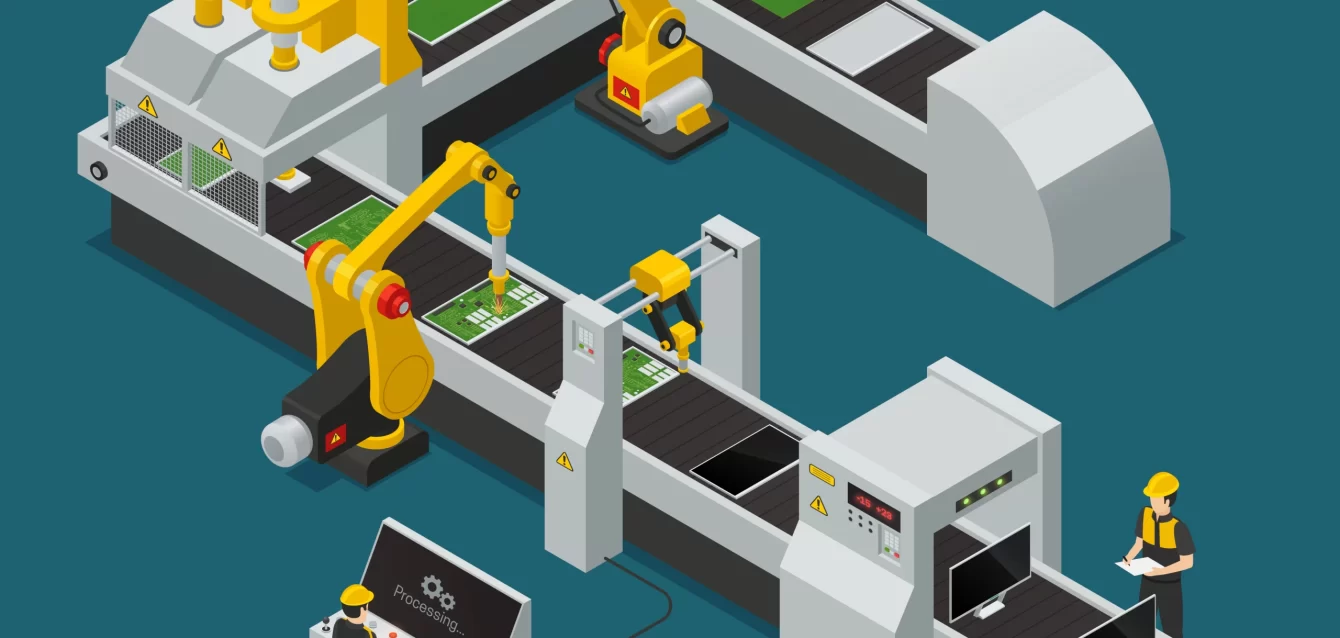
The following stages explain how electronic components are assembled onto a PCB and verified before the board moves into product integration or delivery.
1. Engineering File Review and Design for Manufacturing (DFM)
Before production begins, the assembly team reviews the design and manufacturing files to identify potential assembly problems.
This stage helps prevent component mismatches, placement errors, and manufacturing delays before they reach the production line.
Key activities include:
- Gerber or ODB++ review: Verify PCB layout, pad locations, and fabrication details.
- Bill of Materials (BOM) verification: Check component part numbers, values, package types, and availability.
- Pick-and-place file review: Confirm component coordinates, rotation, and placement orientation.
- Assembly drawing verification: Identify component polarity, special instructions, and mechanical requirements.
- DFM/DFA review: Check whether the design supports reliable manufacturing and component assembly.
A common manufacturing issue is a mismatch between the BOM, PCB footprint, and component package. For example, a component may be electrically correct but physically incompatible with its assigned footprint.
Resolving these inconsistencies before assembly prevents avoidable rework and production interruptions.
2. PCB Preparation and Component Kitting
Once the files are verified, the bare boards and electronic components are prepared for production.
This stage ensures the correct materials are available and suitable for assembly.
- Incoming PCB inspection: Check dimensions, surface finish, solder mask condition, and visible damage.
- Component verification: Match supplied components against the approved BOM.
- Component kitting: Organise components by production requirements and assembly sequence.
- Moisture-sensitive component handling: Follow applicable storage, exposure, and baking requirements.
- ESD protection: Handle sensitive electronic components using appropriate electrostatic discharge controls.
Incorrect components, damaged boards, or improperly handled moisture-sensitive devices can affect assembly quality even when the SMT equipment operates correctly.
3. Solder Paste Application Using a Stencil
Solder paste application is one of the most critical stages in SMT PCB assembly.
A stainless-steel stencil contains openings corresponding to the PCB’s surface-mount pads. Solder paste is printed through these openings to create controlled deposits where components will be soldered.
The process includes:
- Aligning the PCB with the stencil.
- Applying solder paste using a controlled printing process.
- Depositing paste onto the intended component pads.
- Removing the stencil without disturbing the deposits.
- Checking paste alignment and consistency.
Why this stage matters:
- Insufficient solder paste can result in weak or incomplete solder joints.
- Excessive paste can cause solder bridging between adjacent pads.
- Misaligned paste deposits can create component placement and soldering defects.
- Inconsistent printing can affect repeatability across production batches.
For fine-pitch components, stencil design, aperture dimensions, paste selection, and printing conditions require careful control.
4. Solder Paste Inspection (SPI)
After solder paste printing, Solder Paste Inspection evaluates whether the deposits meet the required printing conditions.
SPI systems typically measure solder paste height, area, volume, and position.
This inspection helps identify printing problems before components are placed.
- Detect insufficient or excessive solder paste.
- Identify paste misalignment.
- Check deposit consistency.
- Flag defects for correction before the next stage.
SPI is especially useful for fine-pitch components and repeatable production because it identifies solder paste problems early rather than after soldering.
5. SMT Component Placement Using Pick-and-Place Machines
Once solder paste is applied and verified, surface-mount components are positioned onto the PCB.
Pick-and-place machines use programmed coordinates, feeders, and placement heads to position components accurately on their designated pads.
The process involves:
- Loading components from reels, trays, or other feeders.
- Identifying components using machine vision.
- Placing components at programmed locations.
- Maintaining correct component orientation and polarity.
- Checking placement accuracy against the PCB layout.
What engineers should understand:
- Incorrect component rotation can affect electrical functionality.
- Wrong package selection can create placement incompatibility.
- Placement accuracy becomes increasingly important for fine-pitch devices.
- Component availability and feeder setup can affect production scheduling.
Proper placement allows components to remain positioned correctly during reflow soldering.
6. Reflow Soldering: Forming Reliable Electrical Connections
Reflow soldering permanently connects surface-mount components to the PCB.
The populated board passes through a reflow oven with controlled temperature zones. The solder paste heats, melts, wets the component terminals and PCB pads, and solidifies into solder joints as the board cools.
The process requires a thermal profile suitable for the solder paste, components, and PCB assembly.
Important considerations include:
- Preheating: Gradually increases board temperature and reduces thermal shock.
- Soaking: Helps stabilise temperature across the assembly.
- Reflow: Reaches the temperature required for solder melting and joint formation.
- Cooling: Allows solder joints to solidify under controlled conditions.
An unsuitable reflow profile can result in poor wetting, solder defects, component damage, or thermal stress.
The correct profile depends on component specifications, solder alloy, PCB thermal characteristics, and assembly requirements. A single temperature setting is not suitable for every PCB.
7. Automated Optical Inspection (AOI)
After reflow soldering, Automated Optical Inspection checks the assembled PCB using cameras and image-processing systems.
AOI compares the board against programmed inspection criteria to identify visible assembly defects.
Typical AOI checks include:
- Missing or incorrectly placed components.
- Component misalignment.
- Incorrect component orientation or polarity.
- Visible solder bridging.
- Tombstoning and other visible soldering defects.
- Certain solder joint appearance abnormalities.
AOI helps detect defects quickly and consistently across production batches.
Important limitation: AOI cannot directly inspect solder joints hidden underneath components such as BGAs. These assemblies may require X-ray inspection or additional verification methods.
8. Through-Hole Component Assembly
Some PCBs require components with leads inserted through drilled holes in the board.
Through-hole assembly is commonly used for connectors, larger components, and applications where mechanical or electrical requirements favour leaded components.
The process includes:
- Inserting components into designated PCB holes.
- Checking component orientation and lead positioning.
- Securing components where required.
- Soldering component leads using suitable methods.
- Inspecting solder joints and trimming leads where applicable.
Depending on the board design and production requirements, through-hole soldering may use wave soldering, selective soldering, or manual soldering.
Wave soldering is suitable for boards with compatible through-hole layouts and production requirements.
Selective soldering allows specific through-hole areas to be soldered while limiting exposure to other components.
Manual soldering is useful for certain prototypes, specialised components, and controlled rework operations.
Not every PCB requires through-hole assembly. Many boards use SMT alone, while others combine SMT and through-hole technologies.
9. X-Ray Inspection for Hidden Solder Joints
Some electronic components contain solder joints that cannot be inspected directly using conventional optical cameras.
X-ray inspection is particularly useful for assemblies containing:
- Ball Grid Array (BGA) components.
- Quad Flat No-Lead (QFN) packages.
- Other components with hidden solder connections.
X-ray inspection helps evaluate internal solder joint conditions that are not visible from the board surface.
Depending on the package and inspection criteria, it can identify concerns such as:
- Solder bridging beneath components.
- Inadequate solder distribution.
- Certain voiding conditions.
- Abnormal solder joint patterns.
X-ray is not automatically necessary for every PCB. Its use depends on package types, design complexity, reliability requirements, and inspection plans.
10. Electrical Testing and Functional Verification
Visual inspection confirms many assembly characteristics, but it does not prove that a PCB performs its intended function.
Electrical testing verifies whether the assembled board meets defined electrical or functional requirements.
Common testing methods include:
In-Circuit Testing (ICT)
- Checks electrical connections and selected component characteristics.
- Identifies certain opens, shorts, and component-level faults.
- Usually requires a suitable test fixture and accessible test points.
Flying Probe Testing
- Uses movable probes to test electrical connections.
- Suitable for prototypes and certain low-volume applications.
- Reduces the need for dedicated fixture development.
Functional Testing (FCT)
- Powers the PCB under controlled test conditions.
- Verifies defined product functions and interfaces.
- May include communication, sensor, control, or output checks.
Firmware Programming
- Loads firmware or software onto programmable devices when required.
- Verifies programming status and applicable configuration requirements.
The test strategy should be based on what the product must do, not simply on which testing equipment is available.
11. Cleaning, Conformal Coating, and Final Processing
After inspection and testing, some PCBs require additional processing before they are ready for integration.
These operations depend on the product’s environmental and functional requirements.
- Cleaning: Removes residues when required by the soldering process and product specifications.
- Conformal coating: Provides a protective layer against certain environmental contaminants and moisture exposure.
- Depanelization: Separates individual boards from manufacturing panels when applicable.
- Mechanical inspection: Verifies dimensions, connector fit, and other specified requirements.
- Labeling and traceability: Identifies boards or batches using serial numbers, barcodes, or other records.
- Packaging: Protects assembled boards against handling damage, moisture, and ESD risks as appropriate.
Conformal coating is not a universal requirement. It should be selected based on environmental exposure, material compatibility, inspection access, and product design.
12. Final Quality Verification and Delivery
The final stage confirms that the assembled PCB meets the agreed production and inspection requirements.
Before delivery, the assembly process may include:
- Final visual inspection.
- Review of inspection and electrical test results.
- Verification of required programming or configuration.
- Confirmation of rework and repair records.
- Production batch identification and traceability.
- Protective packaging and shipment preparation.
A complete production record helps engineers identify the manufacturing history of a board and investigate problems if they arise during integration or field operation.
SMT vs Through-Hole PCB Assembly: Which Method Is Used?
The assembly method depends on component design, board layout, electrical requirements, mechanical conditions, and production needs.
| Factor | SMT Assembly | Through-Hole Assembly |
|---|---|---|
| Component mounting | Directly onto PCB surface | Leads inserted through PCB holes |
| Typical components | ICs, resistors, capacitors, compact components | Connectors, leaded components |
| Automation | Highly suitable for automated placement | Depends on insertion and soldering method |
| Board density | Supports compact layouts | Requires additional hole and routing space |
| Mechanical considerations | Depends on component and design | Leaded connections can support certain mechanical requirements |
| Soldering methods | Typically reflow soldering | Wave, selective, or manual soldering |
Many modern electronics use mixed-technology PCB assembly, combining SMT and through-hole components on the same board.
What Determines PCB Assembly Quality?
PCB assembly quality depends on more than the soldering machine or inspection equipment.
The final result is influenced by the interaction between design, materials, process control, and testing.
Key quality factors include:
- PCB design quality: Appropriate footprints, clearances, thermal considerations, and manufacturable layouts.
- Component quality: Correct parts, suitable packaging, and verified sourcing.
- Solder paste control: Correct paste selection, stencil design, and printing consistency.
- Placement accuracy: Correct component positions, rotations, and orientations.
- Thermal process control: Reflow profiles suitable for the board and components.
- Inspection coverage: Appropriate AOI, X-ray, and visual inspection criteria.
- Electrical verification: Testing aligned with product functionality and risk.
- Process traceability: Records that support production monitoring and investigation.
A reliable assembly process combines these controls rather than depending on a single final inspection.
Common PCB Assembly Defects and Their Prevention
Understanding typical assembly defects helps engineers identify where process controls are most valuable.
| Defect | Possible cause | Prevention approach |
|---|---|---|
| Solder bridging | Excess paste, printing errors, or unsuitable pad design | Improve stencil design and paste control |
| Insufficient solder | Inadequate paste deposition or poor wetting | Verify printing and reflow conditions |
| Tombstoning | Uneven soldering forces or thermal imbalance | Review pad design, paste, and thermal profile |
| Component misalignment | Placement errors or paste instability | Verify placement programming and SPI |
| Cold or poorly wetted joints | Unsuitable thermal conditions or surface issues | Review soldering profile and materials |
| Hidden BGA defects | Placement, paste, or reflow-related issues | Use suitable X-ray inspection and process controls |
| Component damage | Incorrect handling or excessive thermal exposure | Follow component handling and process specifications |
The most effective prevention approach is to identify the defect’s root cause and correct the relevant manufacturing stage rather than relying only on final inspection.
How to Prepare for PCB Assembly: A Practical Checklist
Good preparation can reduce clarification cycles, production interruptions, and assembly errors.
Before submitting a PCB for assembly, verify the following:
- Final Gerber or ODB++ fabrication files are available.
- BOM contains correct manufacturer part numbers and quantities.
- Pick-and-place file includes accurate coordinates and rotation.
- Assembly drawings identify polarity and special instructions.
- Component footprints match the selected packages.
- DFM/DFA concerns have been reviewed.
- Critical components and sourcing requirements are identified.
- Programming and functional testing requirements are documented.
- Inspection and quality acceptance criteria are agreed.
- Required traceability and documentation are defined.
Providing accurate manufacturing information helps the assembly team understand the design and establish an appropriate production process.
PCB Assembly Process: From Prototype to Mass Production
The PCB assembly process may remain fundamentally similar across production volumes, but preparation, equipment setup, testing, and cost considerations change.
| Production stage | Main consideration |
|---|---|
| Prototype assembly | Design verification, engineering changes, and flexible testing |
| Low-volume assembly | Repeatability, setup efficiency, and component availability |
| Medium-volume production | Process stability, inspection coverage, and production planning |
| Mass production | Automation, consistency, traceability, and yield monitoring |
A design that works in a prototype may still require manufacturing improvements before scaling.
Common scale-up considerations include:
- Component availability and sourcing consistency.
- Assembly panelisation and handling.
- Test fixture development.
- Production programming and documentation.
- Process repeatability across batches.
- Design changes and revision control.
Planning these requirements early helps avoid unnecessary redesign and production delays.
Frequently Asked Questions About PCB Assembly
What are the main steps in the PCB assembly process?
The main steps are engineering file review, material preparation, solder paste printing, SPI, component placement, reflow soldering, inspection, through-hole assembly when required, electrical testing, and final processing.
What is the difference between PCB manufacturing and PCB assembly?
PCB manufacturing produces the bare circuit board through processes such as copper patterning, drilling, plating, and surface finishing. PCB assembly mounts and solders electronic components onto that fabricated board to create a functional electronic assembly.
Is SMT assembly the same as PCB assembly?
No. SMT is one method of PCB assembly. PCB assembly may include SMT, through-hole technology, or a combination of both.
Why is AOI inspection important in PCB assembly?
AOI detects many visible assembly defects, including missing components, misalignment, incorrect orientation, and certain soldering problems. It improves inspection consistency but cannot directly verify hidden solder joints.
Does every PCB require X-ray inspection?
No. X-ray inspection is generally selected when component packages, hidden solder joints, or product reliability requirements justify it. BGA and certain QFN assemblies are common examples.
What files are required for PCB assembly?
Typical files include Gerber or ODB++ data, a BOM, pick-and-place coordinates, and assembly drawings. Additional information may include test specifications, firmware, special process instructions, and approved component alternatives.
How can PCB assembly quality be improved?
PCB assembly quality can be improved through manufacturable design, accurate BOM and placement data, controlled solder paste printing, suitable reflow profiles, appropriate inspection coverage, and electrical testing aligned with product requirements.
Key Takeaways: Building Reliable Electronics Through PCB Assembly
The PCB assembly process transforms a fabricated circuit board into a functional electronic product through carefully controlled manufacturing and verification stages.
- Design preparation identifies manufacturing risks before production begins.
- Solder paste printing and component placement establish the foundation for reliable SMT assembly.
- Reflow soldering creates electrical and mechanical connections between components and the PCB.
- AOI and X-ray inspection detect different types of assembly defects.
- Electrical testing verifies defined circuit or product functionality.
- Through-hole assembly and additional processing depend on board design and application requirements.
- Traceability and process control support consistent manufacturing and future problem investigation.
Reliable electronics are built through the combination of sound design, suitable materials, controlled assembly processes, and meaningful verification.
Understanding these stages helps hardware engineers make better manufacturing decisions, prepare production-ready designs, and move electronic products from prototype development toward scalable manufacturing with greater confidence.