A PCB may look repaired after rework, but appearance alone does not confirm reliability. Hidden solder defects, component damage, and process-induced issues can still cause field failures, warranty claims, or compliance problems. PCB rework verification techniques help manufacturers confirm that a repaired board meets the same quality standards expected from the original assembly process.
This guide explains the inspection and verification methods used after PCB rework, when each technique is appropriate, and how manufacturers ensure repaired boards are ready for deployment.
Why PCB Rework Verification Matters
PCB rework is often necessary to correct assembly defects, replace damaged components, implement engineering changes, or recover high-value assemblies. However, rework introduces additional thermal and mechanical stress to the board.
Without proper verification, organizations risk releasing products with hidden defects.
Common risks include:
- Solder bridges that are not visible during basic inspection
- Lifted pads or damaged copper traces
- Component misalignment after replacement
- Excessive heat damage to nearby components
- Intermittent electrical failures
- Reduced long-term reliability
A successful rework process is not complete until the repaired area has been thoroughly verified.
What Should Be Verified After PCB Rework?
Verification focuses on confirming both workmanship quality and functional performance.
The goal is to determine whether the board performs as intended without introducing new defects.
Key areas typically verified include:
- Solder joint integrity
- Component placement accuracy
- PCB surface condition
- Electrical continuity
- Functional performance
- Compliance with acceptance criteria
- Reliability of the repaired area
The verification requirements often depend on product complexity, application risk, and industry standards.
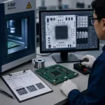
Visual Inspection: The First Verification Step
Visual inspection is usually the first evaluation performed after rework.
Although it is the simplest technique, experienced inspectors can identify many common defects before advanced testing begins.
Inspectors typically evaluate:
- Solder joint appearance
- Component alignment
- Polarity orientation
- Missing components
- Excess solder
- Insufficient solder
- Flux residue
- Surface damage
Visual inspection is effective for obvious defects but cannot reveal hidden issues beneath components or inside solder joints.
For that reason, it is usually combined with additional verification methods.
Microscopic Inspection for Fine-Pitch Components
As PCB density increases, many defects become difficult to detect with the naked eye.
Microscopic inspection provides a closer view of critical areas and helps identify workmanship issues that standard visual checks may miss.
Typical findings include:
- Hairline solder bridges
- Fine-pitch lead defects
- Micro-cracks
- Pad damage
- Solder void indications
- Component lead deformation
This technique is particularly important for:
- QFN packages
- Fine-pitch ICs
- High-density assemblies
- Miniaturized electronics
Microscopic inspection significantly improves defect detection accuracy after rework.
Automated Optical Inspection (AOI)
Automated Optical Inspection compares the repaired assembly against predefined acceptance criteria.
AOI systems rapidly evaluate large numbers of boards while maintaining consistency.
AOI can detect:
- Missing components
- Incorrect component placement
- Polarity errors
- Solder defects
- Dimensional variations
- Component skew
Advantages include:
- Faster inspection cycles
- Repeatable results
- Reduced operator variability
- Improved production throughput
However, AOI remains limited to visible features and cannot inspect hidden solder joints.
X-Ray Inspection for Hidden Defects
Many modern packages contain solder joints that cannot be inspected visually.
X-ray inspection allows manufacturers to evaluate internal solder connections without damaging the assembly.
X-ray systems are commonly used for:
- BGA components
- QFN packages
- Bottom-terminated components
- Multi-layer assemblies
X-ray inspection can reveal:
- Voids
- Solder bridges
- Insufficient solder
- Open connections
- Misaligned balls
- Internal defects
For complex assemblies, X-ray verification is often considered essential after critical rework operations.
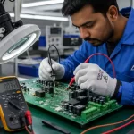
Electrical Testing and Continuity Verification
A board that appears acceptable visually may still contain electrical defects.
Electrical testing verifies that current paths function correctly after rework.
Typical tests include:
- Continuity testing
- Isolation testing
- Resistance measurement
- Power rail verification
- Short-circuit detection
Electrical verification helps identify:
- Broken traces
- Hidden opens
- Unintended shorts
- Damaged interconnections
This step is particularly important when rework involves fine-pitch devices or multilayer boards.
In-Circuit Testing (ICT)
In-Circuit Testing evaluates individual components and circuit sections directly on the PCB.
ICT provides a deeper level of verification than simple continuity testing.
Common checks include:
- Component values
- Connection integrity
- Power distribution
- Signal path validation
- Device presence verification
Benefits include:
- High fault coverage
- Rapid diagnosis
- Repeatable measurements
- Reduced troubleshooting time
ICT is especially useful in production environments where consistency and traceability are critical.
Functional Testing: Verifying Real-World Performance
Even when solder joints and electrical connections pass inspection, the board must still perform its intended function.
Functional testing verifies system-level behavior under operating conditions.
Testing may include:
- Power-up validation
- Signal processing checks
- Communication interface testing
- Sensor validation
- Firmware verification
- Performance measurement
Functional testing answers the most important question:
Does the repaired board work as intended?
For many applications, this is the final acceptance criterion.
Comparing Verification Methods
Different inspection techniques address different types of defects.
No single method provides complete coverage.
| Verification Method | Detects Visible Defects | Detects Hidden Defects | Verifies Function |
|---|---|---|---|
| Visual Inspection | Yes | No | No |
| Microscopic Inspection | Yes | Limited | No |
| AOI | Yes | No | No |
| X-Ray Inspection | Limited | Yes | No |
| Electrical Testing | No | Yes | Partial |
| ICT | Partial | Yes | Partial |
| Functional Testing | No | No | Yes |
The most reliable verification strategy combines multiple techniques rather than relying on a single inspection method.
Common Verification Mistakes After PCB Rework
Verification failures often occur because organizations stop inspection too early.
A visually acceptable board may still contain defects that affect long-term reliability.
Common mistakes include:
- Relying only on visual inspection
- Skipping electrical verification
- Ignoring thermal damage risks
- Failing to inspect nearby components
- Using inconsistent acceptance criteria
- Omitting documentation and traceability
These issues can significantly increase field failure rates.
How to Choose the Right Verification Technique
The appropriate verification method depends on product complexity, risk level, and application requirements.
Higher-risk products require more comprehensive validation.
A practical approach includes:
- Visual inspection for all reworked assemblies
- Microscopic inspection for fine-pitch components
- X-ray inspection for hidden solder joints
- Electrical testing after circuit modifications
- Functional testing before final release
Critical applications often require several verification methods working together.
Key Takeaways
PCB rework verification is about more than confirming a repair was completed. It is about proving the board remains reliable, functional, and compliant with quality requirements.
Important points to remember:
- Visual inspection should always be the starting point
- Hidden solder joints often require X-ray verification
- Electrical testing detects issues that visual checks cannot
- Functional testing confirms real-world performance
- No single inspection method provides complete coverage
- Combining verification techniques produces the most reliable results
- Thorough verification reduces field failures and quality risks
As PCB assemblies become more complex and densely populated, effective verification techniques become increasingly important. Organizations that invest in comprehensive post-rework inspection processes are better positioned to deliver reliable products, reduce costly failures, and maintain consistent quality standards across every board they release.
Frequently Asked Questions
What is the most important inspection method after PCB rework?
There is no single inspection method that works for every situation. Visual inspection is typically the first step, but electrical testing, X-ray inspection, and functional testing are often required to verify the quality and reliability of the repaired board.
Is visual inspection enough to verify PCB rework quality?
No. Visual inspection can identify surface-level defects such as solder bridges, misaligned components, and insufficient solder. However, it cannot detect hidden defects beneath packages like BGAs or confirm electrical performance.
When should X-ray inspection be used after PCB rework?
X-ray inspection is recommended when rework involves hidden solder joints, especially on BGA, QFN, and other bottom-terminated components. It helps identify voids, open connections, and internal solder defects that are not visible externally.
Why is functional testing important after PCB rework?
Functional testing confirms that the repaired PCB performs as intended under operating conditions. A board may pass visual and electrical inspections but still fail when running actual system functions.
Can PCB rework affect long-term reliability?
Yes. Excessive heat exposure, improper soldering, lifted pads, or damage to nearby components can reduce reliability. Proper verification helps identify these issues before the board is released for use.