Introduction
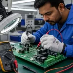
In today’s fast-paced electronics market, speed, quality, and cost-efficiency are crucial to staying competitive. One strategy companies are increasingly adopting is to outsource PCB design to India. Why India? The country has emerged as a hub for electronics design engineering, offering skilled professionals, competitive pricing, and rapid turnaround times without compromising quality.
Outsourcing PCB design allows companies to focus on their core strengths—whether product strategy, marketing, or system integration—while experienced engineers handle complex design work. By leveraging external expertise, businesses can reduce time-to-market, improve design reliability, and optimize manufacturing readiness.
This article explains the entire process of PCB design outsourcing in India. You’ll learn how it works, key technical terms, real-world applications, benefits, and challenges. By the end, you will have actionable insights to decide whether outsourcing PCB design to India is the right move for your business.
What Is PCB Design Outsourcing?
PCB (Printed Circuit Board) design outsourcing is the practice of hiring an external company or engineering team, often in another country, to create a functional PCB design for your product.
Instead of managing an in-house PCB design team, outsourcing allows businesses to:
- Access skilled engineers with deep technical expertise.
- Reduce operational costs.
- Accelerate time-to-market by leveraging ready-to-work teams.
Technical Terms You Need to Know
- Schematic Design: Blueprint showing how components are connected.
- PCB Layout: Physical placement of components on the board.
- Signal Integrity (SI): Ensuring electrical signals travel correctly.
- Electromagnetic Compatibility (EMC): Preventing interference with other devices.
- Design for Manufacturing (DFM): Designing the PCB so it can be efficiently and reliably produced.
- BOM (Bill of Materials): Complete list of components used in the PCB design.
How Does PCB Design Outsourcing Work?
Outsourcing PCB design involves several structured steps that ensure efficiency, quality, and manufacturability.
Step 1: Requirement Gathering
A detailed understanding of your product’s functional and technical needs is essential. You should provide:
- Circuit schematics.
- Desired PCB dimensions and form factor.
- Performance specifications.
- Special constraints (thermal, mechanical, or regulatory).
Step 2: Conceptual Design
Engineers create block diagrams representing the functional modules. Key considerations include:
- Power Distribution: Ensuring consistent voltage levels to all components.
- Signal Routing: Proper trace paths to minimize crosstalk and signal loss.
- Thermal Management: Identifying hotspots and optimizing heat dissipation.
- Component Selection: Ensuring availability and compliance with standards.
Step 3: PCB Layout & Routing
- Components are placed strategically for optimal performance and manufacturability.
- Routing is done layer by layer using software like Altium Designer, KiCAD, or OrCAD.
- Special attention is given to high-speed traces, impedance control, and via placement.
Step 4: Simulation and Validation
Before finalizing the design, engineers perform:
- DRC (Design Rule Check): Ensures design adheres to manufacturing capabilities.
- Signal Integrity Analysis: Verifies high-speed signals remain undistorted.
- Thermal Simulation: Confirms the board can handle expected heat loads.
- EMC Testing: Minimizes interference with nearby devices.
Step 5: Handoff to Manufacturing
The final deliverables include:
- Gerber Files: Standard format for PCB manufacturing.
- BOM (Bill of Materials): For sourcing components.
- Assembly Instructions: Ensuring correct production.
- Test Plans: Guidelines for functional testing after assembly.
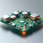
Key Components in PCB Design
| Component | Function | Technical Note |
|---|---|---|
| Resistor | Controls current | Measured in ohms (Ω), can affect voltage drop |
| Capacitor | Stores/releases energy | Used for filtering, decoupling, and timing |
| Inductor | Stores energy in magnetic field | Used in power circuits, filters, and EMI suppression |
| IC (Integrated Circuit) | Performs complex functions | Can include microcontrollers, amplifiers, sensors |
| Trace | Conductive path | Width and thickness determine current capacity |
| Via | Connects different layers | Can be through-hole, blind, or buried |
| PCB Layers | Multiple conductive layers | Multi-layer boards support complex circuitry |
Tip: A well-designed PCB ensures minimal noise, optimal signal integrity, and long-term reliability of the product.
Real-Life Applications
Outsourced PCB designs are used across industries, from consumer electronics to aerospace. Examples:
- Consumer Electronics: Smartphones, smartwatches, IoT devices, and smart home gadgets.
- Industrial Automation: PLC controllers, sensor modules, and motor drivers.
- Medical Devices: ECG monitors, diagnostic tools, and wearable biosensors.
- Aerospace & Defense: Drones, avionics systems, radar, and satellite electronics.
- Automotive Electronics: Electric vehicle battery management systems, infotainment, and Advanced Driver-Assistance Systems (ADAS).
Outsourcing allows companies to access specialized PCB design expertise required for advanced products like multi-layer high-speed boards, RF circuits, or IoT connectivity modules.
Benefits of Outsourcing PCB Design to India
1. Cost-Effective Solutions
- India offers competitive engineering rates without compromising on quality.
- Reduces costs associated with hiring full-time staff, training, and infrastructure.
2. Access to Skilled Engineers
- India has a large pool of engineers with experience in signal integrity, thermal management, high-speed circuits, and embedded systems.
- Engineers are familiar with international standards like IPC, ISO, CE, and RoHS compliance.
3. Faster Turnaround
- Experienced teams can deliver designs quicker than an in-house team starting from scratch.
- Parallel workflows reduce time-to-market.
4. Scalability
- You can scale your design resources as per project complexity and deadlines.
5. Focus on Core Business
- Outsourcing allows your team to concentrate on product innovation, strategy, and marketing.
Challenges and How to Overcome Them
While outsourcing has advantages, it comes with challenges:
| Challenge | How to Overcome |
|---|---|
| Communication Gaps | Use video calls, detailed specs, and frequent updates |
| Time Zone Differences | Overlap working hours for key meetings |
| IP Security | Sign NDAs and legal contracts to protect intellectual property |
| Quality Variation | Choose verified service providers with proven track records |
Pro Tip: Use project management tools like Trello, Jira, or Asana to track design progress and maintain accountability.
Best Practices for Successful PCB Design Outsourcing
- Define Clear Requirements: Provide detailed schematics, dimensions, and performance expectations.
- Select Experienced Partners: Verify past projects, certifications, and client reviews.
- Use Standardized Documentation: Ensure Gerber files, BOMs, and assembly instructions are precise.
- Perform Regular Reviews: Check layouts, DRC reports, and simulations periodically.
- Protect IP: Establish legal safeguards before sharing designs.
Conclusion
Outsourcing PCB design to India is a strategic choice for companies aiming to reduce costs, accelerate development, and leverage technical expertise. By following structured workflows, selecting experienced partners, and focusing on clear communication, businesses can achieve high-quality, reliable designs. From consumer electronics to industrial automation and medical devices, Indian PCB designers offer practical, cost-effective solutions that help bring products from concept to market faster.
Take action today: partner with a professional PCB design service in India and experience faster development cycles, optimized performance, and a competitive edge in the global electronics market.